- 您现在的位置:买卖IC网 > Sheet目录2007 > LTC6994CDCB-2#TRPBF (Linear Technology)IC DELAY LINE 6-DFN
LTC6994-1/LTC6994-2
20
699412fb
699412 F16
LTC6994
IN
GND
SET
OUT
V+
DIV
C1
0.1F
R1
R2
RSET
V+
DIV
SET
OUT
GND
IN
C1
R1
R2
V+
RSET
DCB PACKAGE
IN
GND
SET
OUT
V+
DIV
R2
V+
RSET
TSOT-23 PACKAGE
R1
C1
applicaTions inForMaTion
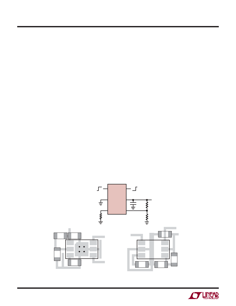
Figure 16. Supply Bypassing and PCB Layout
Supply Bypassing and PCB Layout Guidelines
TheLTC6994isanaccuratemonostablemultivibratorwhen
used in the appropriate manner. The part is simple to use
and by following a few rules, the expected performance is
easily achieved. Adequate supply bypassing and proper
PCB layout are important to ensure this.
Figure 16 shows example PCB layouts for both the SOT-23
and DCB packages using 0603 sized passive components.
The layouts assume a two layer board with a ground plane
layer beneath and around the LTC6994. These layouts are
a guide and need not be followed exactly.
1. Connect the bypass capacitor, C1, directly to the V+ and
GND pins using a low inductance path. The connection
from C1 to the V+ pin is easily done directly on the top
layer. For the DCB package, C1’s connection to GND is
also simply done on the top layer. For the SOT-23, OUT
can be routed through the C1 pads to allow a good C1
GND connection. If the PCB design rules do not allow
that,C1’sGNDconnectioncanbeaccomplishedthrough
multiple vias to the ground plane. Multiple vias for both
the GND pin connection to the ground plane and the
C1 connection to the ground plane are recommended
to minimize the inductance. Capacitor C1 should be a
0.1F ceramic capacitor.
2. Place all passive components on the top side of the
board. This minimizes trace inductance.
3. Place RSET as close as possible to the SET pin and make
adirect,shortconnection.TheSETpinisacurrentsum-
ming node and currents injected into this pin directly
modulate the output delay. Having a short connection
minimizes the exposure to signal pickup.
4. Connect RSET directly to the GND pin. Using a long path
or vias to the ground plane will not have a significant
affect on accuracy, but a direct, short connection is
recommended and easy to apply.
5. Use a ground trace to shield the SET pin. This provides
another layer of protection from radiated signals.
6. Place R1 and R2 close to the DIV pin. A direct, short
connection to the DIV pin minimizes the external signal
coupling.
发布紧急采购,3分钟左右您将得到回复。
相关PDF资料
LTC7541ABN#PBF
IC CMOS D/A CONV 12BIT 18-DIP
LTC7545ACG#TRPBF
IC D/ACONV MULTIPLY 12BIT 20SSOP
LTC8043EN8
IC D/A CONV 12BIT SERIAL 8-DIP
LTC8143ESW#TRPBF
IC D/A CONV 12BIT SERIAL 16-SOIC
LTM9011CY-14#PBF
IC ADC 14BIT UMODULE 140BGA
LV5609LP-E
IC CLOCK DRIVER VERTICAL 24VCT
LV5609LP-TE-L-E
IC CLOCK DRIVER VERT VCT24
M-986-2A1PL
IC TRANSCEIVER MF 2CHAN 44-PLCC
相关代理商/技术参数
LTC6994CDCB-2TRMPBF
制造商:LINER 制造商全称:Linear Technology 功能描述:TimerBlox: Delay Block/ Debouncer
LTC6994CS6-1#PBF
制造商:Linear Technology 功能描述:SC-Timing, Cut Tape Delay with Rising or Falling Edge Trigger
LTC6994CS6-1#TRMPBF
功能描述:IC DELAY LINE TSOT-23-6 RoHS:是 类别:集成电路 (IC) >> 时钟/计时 - 延迟线 系列:TimerBlox® 标准包装:2,500 系列:- 标片/步级数:- 功能:多个,不可编程 延迟到第一抽头:10ns 接头增量:- 可用的总延迟:10ns 独立延迟数:4 电源电压:4.75 V ~ 5.25 V 工作温度:0°C ~ 70°C 安装类型:表面贴装 封装/外壳:14-SOIC(0.154",3.90mm 宽) 供应商设备封装:14-SOIC 包装:带卷 (TR)
LTC6994CS6-1#TRPBF
功能描述:IC DELAY LINE TSOT-23-6 RoHS:是 类别:集成电路 (IC) >> 时钟/计时 - 延迟线 系列:TimerBlox® 标准包装:2,500 系列:- 标片/步级数:- 功能:多个,不可编程 延迟到第一抽头:10ns 接头增量:- 可用的总延迟:10ns 独立延迟数:4 电源电压:4.75 V ~ 5.25 V 工作温度:0°C ~ 70°C 安装类型:表面贴装 封装/外壳:14-SOIC(0.154",3.90mm 宽) 供应商设备封装:14-SOIC 包装:带卷 (TR)
LTC6994CS6-1TRMPBF
制造商:Linear Technology 功能描述:Delay Block/Debouncer 1us-33.6s TSOT23-6
LTC6994CS6-2#PBF
制造商:Linear Technology 功能描述:DELAY BLOCK/DEBOUNCER 5.5V T 制造商:Linear Technology 功能描述:DELAY BLOCK/DEBOUNCER, 5.5V, TSOT-23-6; Operating Mode:Monostable; Supply Voltage Min:2.25V; Supply Voltage Max:5.5V; Digital IC Case Style:TSOT-23; No. of Pins:6; Clock External Input:Yes; Operating Temperature Min:0C ;RoHS Compliant: Yes
LTC6994CS6-2#TRMPBF
功能描述:IC DELAY LINE TSOT-23-6 RoHS:是 类别:集成电路 (IC) >> 时钟/计时 - 延迟线 系列:TimerBlox® 标准包装:2,500 系列:- 标片/步级数:- 功能:多个,不可编程 延迟到第一抽头:10ns 接头增量:- 可用的总延迟:10ns 独立延迟数:4 电源电压:4.75 V ~ 5.25 V 工作温度:0°C ~ 70°C 安装类型:表面贴装 封装/外壳:14-SOIC(0.154",3.90mm 宽) 供应商设备封装:14-SOIC 包装:带卷 (TR)
LTC6994CS6-2#TRPBF
功能描述:IC DELAY LINE TSOT-23-6 RoHS:是 类别:集成电路 (IC) >> 时钟/计时 - 延迟线 系列:TimerBlox® 标准包装:2,500 系列:- 标片/步级数:- 功能:多个,不可编程 延迟到第一抽头:10ns 接头增量:- 可用的总延迟:10ns 独立延迟数:4 电源电压:4.75 V ~ 5.25 V 工作温度:0°C ~ 70°C 安装类型:表面贴装 封装/外壳:14-SOIC(0.154",3.90mm 宽) 供应商设备封装:14-SOIC 包装:带卷 (TR)